Historic FirstFirst private finishing training institute in India to tape out real silicon — GF180nm · Synopsys powered SNUG IndiaRecognised by Synopsys at SNUG India — 9 students · 3 teams · 3.5 months Cohort 2Next ChipTapeout cohort being planned — register interest: +91 97400 33323 Historic FirstFirst private finishing training institute in India to tape out real silicon — GF180nm · Synopsys powered SNUG IndiaRecognised by Synopsys at SNUG India — 9 students · 3 teams · 3.5 months Cohort 2Next ChipTapeout cohort being planned — register interest: +91 97400 33323
Overview Workforce Development Events & Recognition ChipTapeout Articles
🏆 Industry First — Private Training Institute in India

Real Silicon.
Real Students.
Real Achievement.

VLSI EXPERT's ChipTapeout program takes students from Tier 2 and Tier 3 colleges through a complete chip design and fabrication cycle — RTL to GDSII to real silicon — using Synopsys EDA tools on GlobalFoundries GF180nm process. We are the first private finishing training institute in India to do this.

🏭 GlobalFoundries GF180nm 🛠 Full Synopsys toolchain 🏆 Recognised at SNUG India
1st
Private Training Institute
in India to tape out
🎓
Cohort 1 — 20269 students · Mini Processor
🏭
GF180nmReal silicon fabrication
3.5 monthsRTL to tapeout
🏆
SNUG IndiaSynopsys recognition
9
Students Cohort 1
GF180
nm Process Node
3.5
Months RTL→Silicon
SNUG
India Recognition
1st
Private Institute India
What is a Chip Tapeout?

From RTL on a screen to silicon in your hand.

A tapeout is the complete journey — writing RTL, simulation, synthesis, physical design, signoff, and submitting to a foundry for fabrication. Every step done with industry-standard Synopsys tools under real design constraints.

01
RTL Design
Write hardware RTL — the logic that defines what the chip does.
Synopsys VCS
02
Simulation & Verification
Simulate RTL, build testbenches, verify functional correctness.
VCS · Verdi
03
Synthesis
Convert RTL to gate-level netlist targeting GF180nm cell library.
Design Compiler
04
Physical Design
Floorplan, place, route, clock tree. Full physical implementation.
IC Compiler II
05
Signoff
STA, DRC, LVS — all clean before the foundry accepts the file.
PrimeTime
06
Fabrication
GDSII submitted to GlobalFoundries. Silicon returns 8–12 weeks later.
GlobalFoundries GF180nm
ChipTapeout Cohort 1 — 2026

Nine students. One chip. A historic first.

In 3.5 months, nine students from Tier 2 and Tier 3 colleges designed a Mini Processor, taped out on GF180nm, and were recognised by Synopsys at SNUG India. No private training institute had done this before — anywhere in India.


✓ Completed · Silicon Received
Mini Processor · GF180nm · Cohort 1
A. Srujan Reddy · Santosh Yadav · Renisha · Anjanay Vatsa · Ritik Kumar · Tushar Prajapati · Alan Alex · Amarkant · Ruchita Suthar
Sponsored by
SynopsysSynopsys
GlobalFoundriesGF
A. Srujan Reddy
A. Srujan Reddy
Gokaraju Rangaraju Institute of Engineering and Technology · Hyderabad
Physical Design
Santosh Yadav
Santosh Yadav
IIMT College of Engineering · Greater Noida
Physical Design
Renisha
Renisha
St. Joseph's College of Engineering · Chennai
Physical Design
Anjanay Vatsa
Anjanay Vatsa
Birla Institute of Technology Mesra · Ranchi
Frontend Verification
Ritik Kumar
Ritik Kumar
Galgotias University · Greater Noida
Frontend Verification
Tushar Prajapati
Tushar Prajapati
Noida Institute of Engineering and Technology · Noida
Frontend Verification
Alan Alex
Alan Alex
Rajagiri School of Engineering and Technology · Kochi
PDK
Amarkant
Amarkant
IIT (ISM) Dhanbad . Dhanbad
PDK
Ruchita Suthar
Ruchita Suthar
Ganpat University — UV Patel College of Engineering · Ahmedabad
PDK
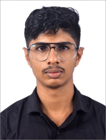
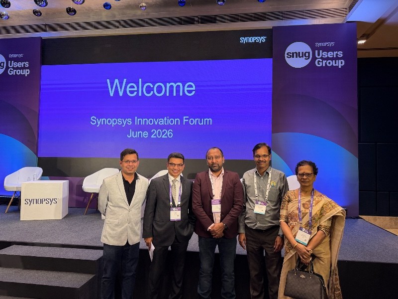
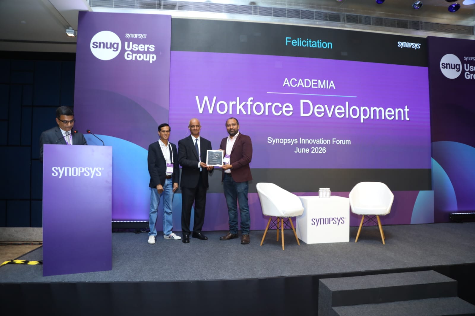
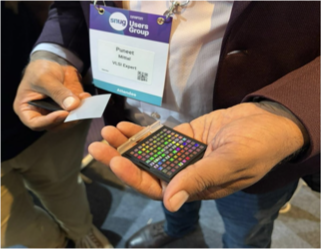
Team group photo SNUG recognition The fabricated chip
Read the full story →
Design
Mini Processor
Process Node
GlobalFoundries GF180nm
Duration
3.5 months
Simulation
Synopsys VCS
Physical Design
Synopsys IC Compiler II
Timing Signoff
Synopsys PrimeTime
Waveform Debug
Synopsys Verdi
Student Background
Tier 2 & Tier 3 colleges only
🏆 Synopsys SNUG India
Recognised by Synopsys at SNUG India — the industry's premier EDA user conference. First private training institute in the country to receive this recognition for a student tapeout program.
Mentors
Puneet Mittal
Overall Execution · PDK Mentoring
Dr. Kanika Nagpal
Program Lead · PD Mentoring
Vyom Sharma
ASIC Verification Mentoring
Industry Mentor
STA Signoff · 7 yrs experience
Industry Mentor
Mixed-Signal ASIC · IO Interface · 15 yrs
Full Story & Details →
Next Program

Cohort 2 is being planned.

Cohort 1 proved it is possible. Cohort 2 will go further — more students, more complex design, same commitment to real silicon. Register your interest now to be considered first.

Cohort 2 — Coming Soon
ChipTapeout Intensive — Cohort 2
Full RTL to GDS flow — Synopsys tools, GlobalFoundries fabrication. Students from Tier 2 & Tier 3 colleges only. Applications open once Cohort 2 details are confirmed.
Why This Is Different

Three things that make this unlike anything else.

1st
No Training Institute Had Done This in India
Chip fabrication happens at IITs, NITs and semiconductor companies. Never at a private finishing training institute — until VLSI EXPERT. With Tier 2 and Tier 3 students, not IIT graduates.
100%
Real Tools. Real Process. Real Silicon.
Not a simulation. Not an FPGA. The same Synopsys tools that production teams use, the same GF180nm process that real chips are made on — and a physical IC at the end.
Tier 2/3
Any College. Any Background.
Every student in Cohort 1 came from a Tier 2 or Tier 3 engineering college. None had prior tapeout experience. With the right mentorship and tools — college name doesn't matter.
Partner or participate?
ChipTapeout Cohort 2 is coming.
Register Interest → View Partnerships