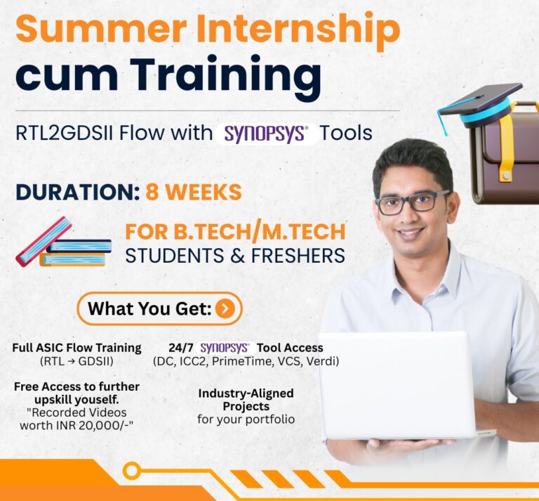
At VLSI EXPERT®, we believe that true learning happens when knowledge meets application. That’s why our Training cum Internship programs are carefully designed to give students and fresh graduates the technical depth, hands-on skills, and real-world exposure they need to thrive in the semiconductor industry.
Our Training cum Internship model combines structured classroom-style learning with hands-on project implementation, allowing participants to build industry-relevant skills while working on practical problems using industry-standard tools like those from Synopsys.
It’s the best of both worlds: Comprehensive Training Modules + Real Project-Based Internship Experience
> Students looking to upskill during their semester breaks
> Freshers preparing for VLSI core roles
> Anyone interested in exploring career opportunities in chip design, layout, or verification
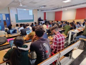
1. Live Instructor-Led Training Sessions
2. Access to Licensed Synopsys Tools for practice
3. Premium Recorded Content for Revision
4. Mentor Support for Project Work
5. Industry-Oriented Assignments & Projects
6. Internship Certificate on successful completion
7. Career Guidance & Resume Review (in some batches)
Unlike many internship programs that are theory-heavy or tool-limited, we provide access to commercial-grade Synopsys tools and real project environments — ensuring you’re job-ready from Day 1.
Clear understanding of VLSI design flow or Custom design flow (Based on Internship Topic)
Exposure to the kind of work done in actual semiconductor companies
Internship Certificate that adds weight to your resume
Confidence to crack technical interviews.
We run Training cum Internship programs twice a year:
Winter Batch: December – January- Feb
Summer Batch: May – June - July
Check the current openings and eligibility criteria before applying.
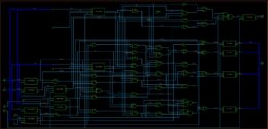
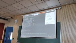
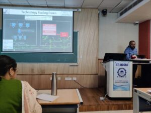
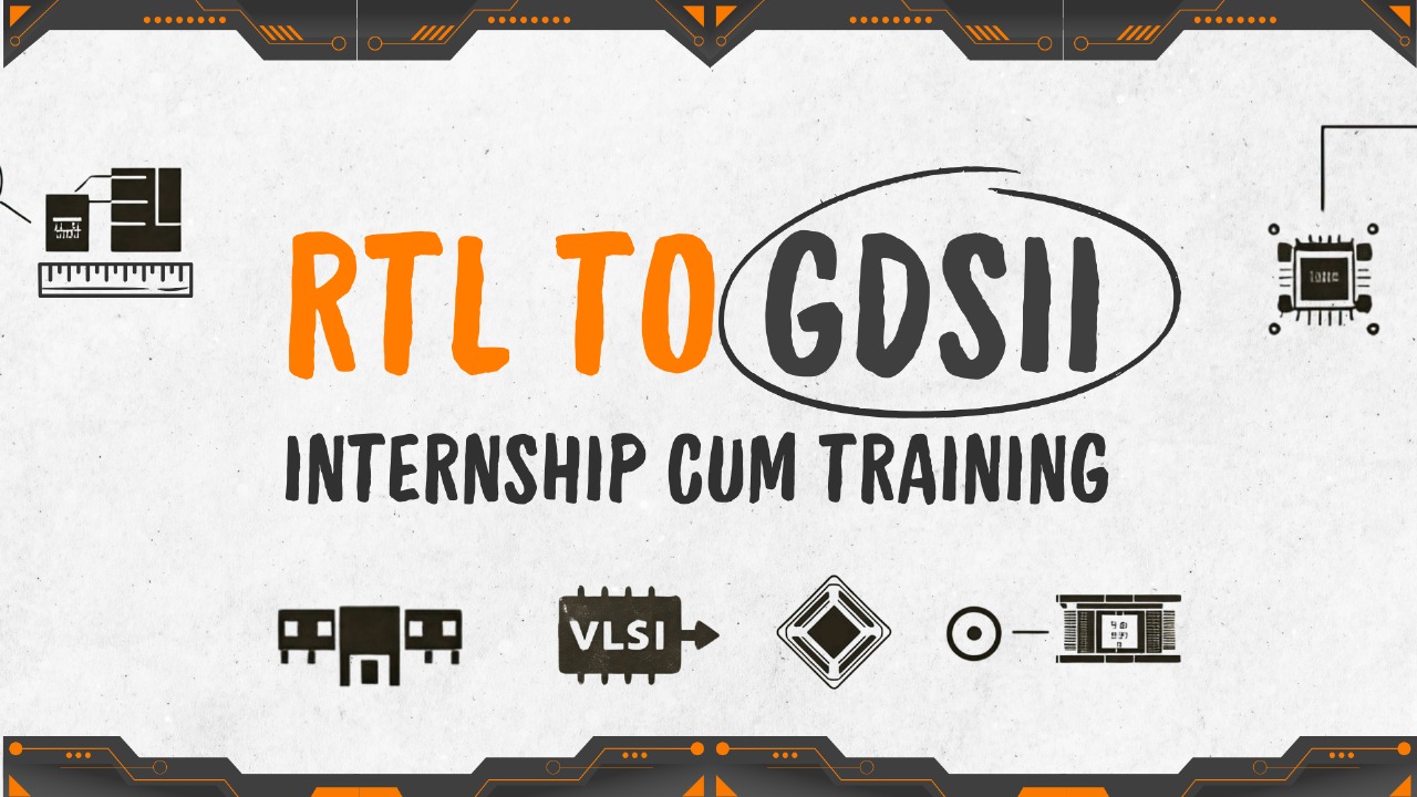
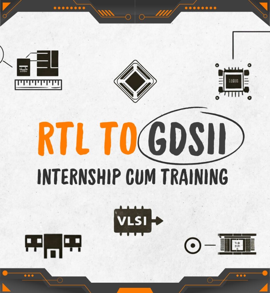
Internship program titled "Physical Design RTL to GDSII Internship cum Training" is meticulously crafted to provide students with a comprehensive understanding of industry-standard practices in RTL to GDS flow within the Synopsys Tool Environment, helping them in Mastering Backend Flow Design.
The internship curriculum is structured to cover essential aspects such as RTL Design, Logic Synthesis, Floorplan-Powerplan, Place and Route & Static Timing Analysis (STA), offering a holistic approach to mastering the semiconductor design process.
The goal is to bridge the gap between theoretical concepts and practical application, ensuring that participants not only grasp fundamental principles but also gain proficiency in utilizing industry-standard tools and methodologies.
Customized & Structured curriculum that covers essential topics in physical design, ensuring a comprehensive learning experience.
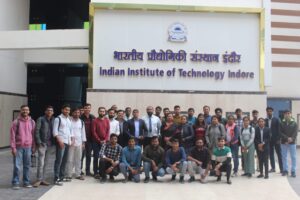
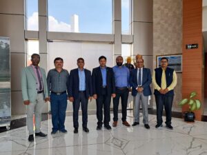
Students will get an opportunity to learn and interact with VLSI Industry professionals.
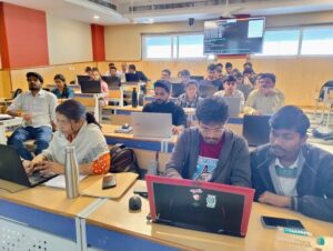
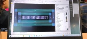
Hands-On Training on Synopsys Tools – which is an Industry Standard Tools.
The sessions will be “Interactive”, it will be learning with practical experience.
This Training Program helps them to get ready for VLSI Industry.
Career Guidance will be provided during or after the Training program.
Project based Design assignments which can be finished within a stipulated timeframe of the Internship.
24*7 Synopsys Tool access for entire Duration of Internship.
Help them to work on a real Project with a real deadline.
Help them to improve their presentation skills and communication skills.
Certification of Training/Workshop on company letter head
Industrial Exposure and Practical knowledge to all participants
All classes are recorded, and access to those recordings is provided using VLSI EXPERT’s internal portal.
Extra Tool access for 2 weeks post Internship.
Module Name | Sub-Topics |
VLSI Flow Introduction (RTL to GDS)
| · RTL TO GDS Flow -VLSI Frontend Design Flow -VLSI Backend Design Flow · Logic Synthesis Concepts · Timing Optimization during Logic Synthesis · Floorplan Overview · Power Planning Overview · Placement Overview · Physical Verification Overview · Routing Overview |
Input output Files. (PDK Files Demystified) | · Liberty (.lib) file · Power constraint, UPF file · Lef/Def, · Spice netlist, · Verilog netlist, Gate level netlist · SDC, SDF, SPEF · ITF file, Tech file · Tluplus file, Nxtgrd file |
Unix and Bash Scripting | · Basic Unix Commands · VI Editor · Bash Scripting |
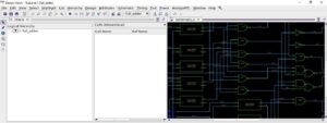
Verilog basic and RTL Designing | · Basic Verilog Syntax · RTL design and Testbench using Verilog. · RTL Simulations and debugging · RTL level partitions · Hierarchical design and flat design · Simulation using VCS and Verdi Tool |
Project | · 2 Projects in which you need to write a Verilog RTL and Simulate using VCS/Verdi · Same RTL we will use in further Physical Design |
Static Timing Analysis | · Delay Concepts (Cell Delay and Gate Delay) · Timing Paths · Timing Arc and .Lib File details · How Timing Tool do the delay calculation · Timing Checks (Setup and Hold; DRV) · Timing Reports · Timing Violations and Methods to Fix Violations |
Timing Constraints | · Clock Constraints · Input output Constraints · How to write Constraints for an RTL |
Logic Synthesis | · Logics Synthesis Overview · Technology File Overview and Mapping · RTL Synthesis using Design Compiler · Optimization techniques during Synthesis · Floorplan aware Synthesis |
Project | · RTL to Gate-level Netlist in different Timing Constraints using Design Compiler · Using the RTL during the RTL module – Map it with Technology Files in different constraint environment using Design Compiler |
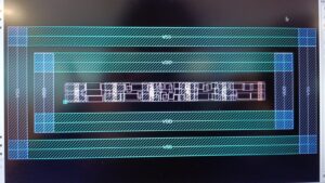
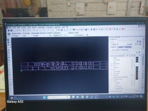
FloorPlan | · Different Physical Constraints – Pin/Ports Constraints · Floorplan Concepts · Floorplan shapes (T, U, L, Rectangle, and Square) & impact of Physical Constants · Macros concepts, Flylines concepts · Hallos, Keepout margins · Utilization Factor, Aspect Ration |
Power Plan | · Power Stripts – VDD/ VSS Rails · Power Mesh · Power Ring |
Projects | · Floorplan and Power Plan concepts implementation using ICC2 |
Placement | · Placement Blockages · Physical Only Cells, Spare Cells, ENDCAP Cells, TieHigh, TieLow cells, Tap Cells, Nwell Cells, DCAP Cells · Course Placement, Legalize Placement · Congestion Concepts · Standard Cell Concepts |
CTS | · Clock Tree Concepts · Concurrent Clock and Data Signal Routing · NDR Rules · Clock Skew, Clock jitter, Clock Network Delay, Clock Latency · H-Tree, Balance Tree , Clock Meshing · Effect of Clock Skew on Timing Checks |
Projects | · Placement of Synthesized Netlist using the Floorplan done in previous Module |
Routing | · Global Routing · Track Routing · Detailed Routing · Routing Tracks, Pitch · |
Parasitic Extraction | · Metal Layer Concepts · Foundry Tech Files · TluPlus Files and Nxtgrd Files · RC concepts and SPEF Files |
Timing Signoff | · Advance Timing Concepts · Fixing of Timing using ECOs · Signal Integrity Concept |
Projects | · Routing using the ICC2 Tools · Parasitic Extraction using StarRC Tools · Timing SignOff using the Primetime Tools |
Project Review and Doubt Clearing | |
Placement Related Sessions | · Mock Interview · Resume Preparation |
VLSI EXERT PVT. LTD. will provide the necessary resources like S/W, Online access, or other required kit.
During the Training, few projects would be undertaken that would be completed by the students.
Completion of Project/s assigned to respective students/group of students are mandatory for completion of the training program.
After completion of the Training program certificates will be awarded by VLSI EXERT PVT. LTD.
Project need to be submitted by every student by the end of the Internship cum Training Program with proper Project Report
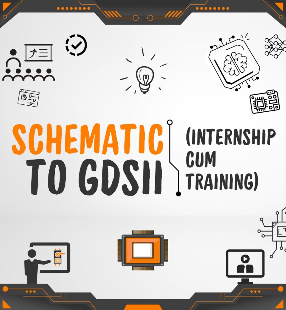
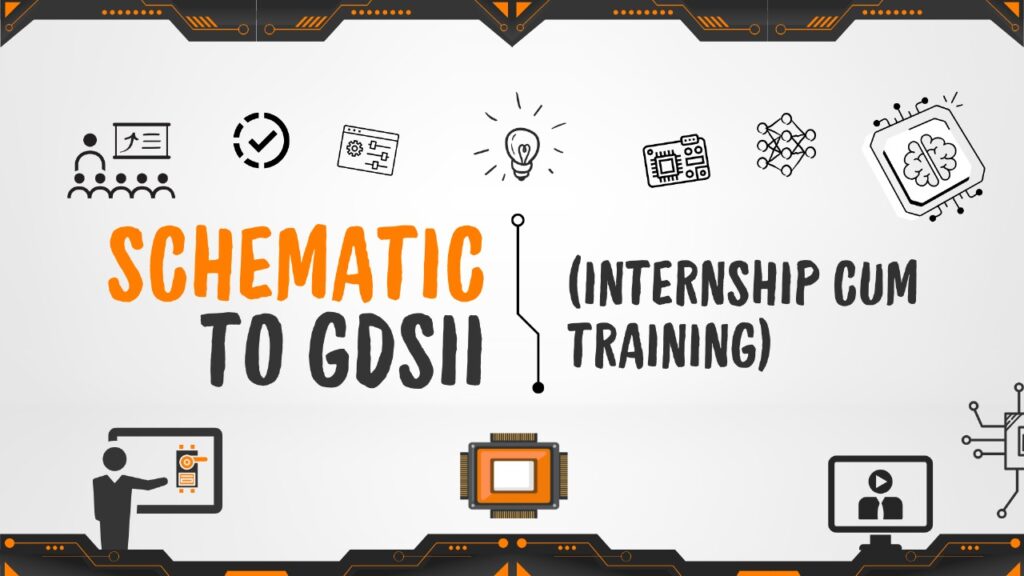
Internship program titled "Physical Design RTL to GDSII Internship cum Training" is meticulously crafted to provide students with a comprehensive understanding of industry-standard practices in Schematic to GDS flow using the Synopsys Tool Environment, helping them in Mastering Custom Flow Design.
The internship curriculum is structured to cover essential aspects such as Schematic Design, Simulation of Circuit, Layout Design, Understanding of PVT Corenrs, LVS and DRC concepts at Standard Cell Design level.
The goal is to bridge the gap between theoretical concepts and practical application, ensuring that participants not only grasp fundamental principles but also gain proficiency in utilizing industry-standard tools and methodologies.
Customized & Structured curriculum that covers essential topics in physical design, ensuring a comprehensive learning experience.
Students will get an opportunity to learn and interact with VLSI Industry professionals.
Hands-On Training on Synopsys Tools – which is an Industry Standard Tools.
The sessions will be “Interactive”, it will be learning with practical experience.
This Training Program helps them to get ready for VLSI Industry.
Career Guidance will be provided during or after the Training program.
Project based Design assignments which can be finished within a stipulated timeframe of the Internship.
24*7 Synopsys Tool access for entire Duration of Internship.
Help them to work on a real Project with a real deadline.
Help them to improve their presentation skills and communication skills.
Certification of Training/Workshop on company letter head
Industrial Exposure and Practical knowledge to all participants
All classes are recorded, and access to those recordings is provided using VLSI EXPERT’s internal portal.
Extra Tool access for 2 weeks post Internship.
VLSI EXERT PVT. LTD. will provide the necessary resources like S/W, Online access, or other required kit.
During the Training, few projects would be undertaken that would be completed by the students.
Completion of Project/s assigned to respective students/group of students are mandatory for completion of the training program.
After completion of the Training program certificates will be awarded by VLSI EXERT PVT. LTD.
Project need to be submitted by every student by the end of the Internship cum Training Program with proper Project Report