Foundation of VLSI Design

VLSI EXPERT / Foundation of VLSI Design

 
Duration:   Approx. 6 Months to 8 Months
Batch Size:    Approx. 20 candidates
Tool Uses:   Synopsys (Industry Standard)
Placement Record:  200+
Mode of Delivery:  LIVE (Instructor-Led)
Mock Interview:   To prepare you for Real Interview
Resume building:  Special Sessions for Resume writing skills.
Assessments:   50+ Assignments
Practice Test:   50+ Online Practice Tests
Projects:   Industry Standard Projects

ECE/EEE students of the following years

  • B.E./B.Tech.  2nd Year, 3rd year, 4th year
  • M.E./M.Tech. 1st Year, 2nd year
  • Pass-out candidates


  • Overview
  • Curriculum
  • Instructor
  • FAQ’s
  • Module Details

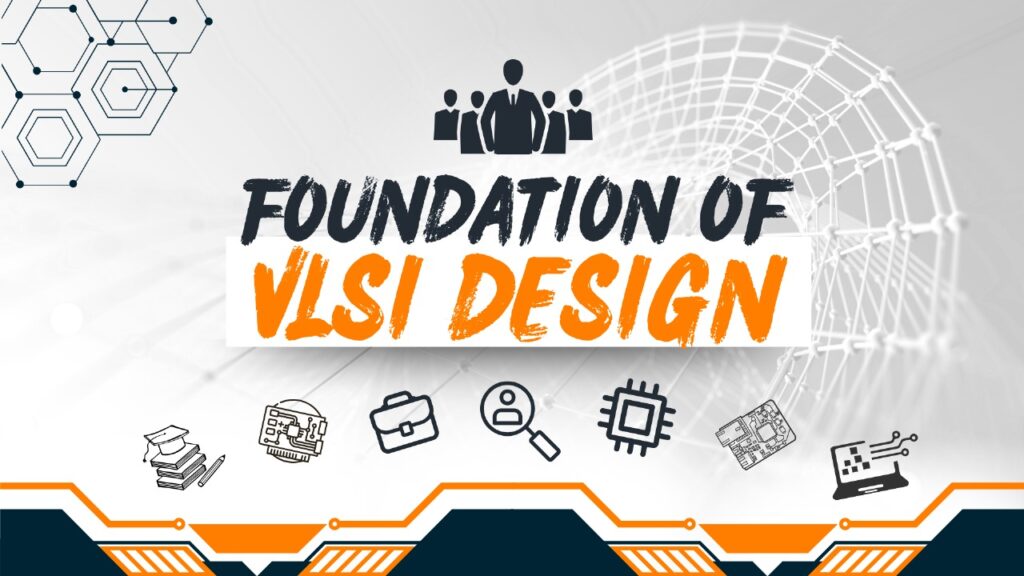
This is basic course offered by VLSI Expert since its inception. This course has been designed by the Industry Experts to develop the skillsets in the candidates which are required by the core VLSI companies at the entry level. It is best suited for Third year and Final Year pass-out B.Tech. Graduates and also for First year and Second year M.Tech. Postgraduates. 

Course has been divided into 2 Levels and 5 Segments. Level 1 is common to all students (Duration is around 2.5Months to 3Months) and Level 2 (which is a profile specific – means you have to choose 1 out of given options). 

Apart from this we understand that there are multiple profiles within the core company and the freshers can be taken into any of the profiles, so we make sure that our candidates get the complete knowledge of all the domain in general.

When it comes to selection in the VLSI Core companies the first step is the written test in which basic aptitude and C is asked and so we also have included a course by the name of ADD ONS. 

This course has been structured in 5 different Segments:

Segment 1: Fundamental & Industrial Implementation (level 1)

  • Topics (which you have studied as part of your B.E./M.E./M.Tech. course curriculum) from VLSI/Semiconductor Industry & Implementation point of view.
  • All the position/profile in VLSI Industry require in-depth understanding of topics. Few of them (from in-depth aspect) are not part of undergraduate program. So, as a part of this Segment – we also fill those gaps as per Industry Requirement.
  • In our UG program, sometime very difficult to co-relate different topics/subjects with each other. That’s the one of the main goals of this Segment.
  • Module Covers
    1. Digital basics to Industrial Digital Design
    2. Semiconductor Theory & Device Physics
    3. CMOS Technology (Fundamental, Designing & Fabrication)
    4. Digital Design using Verilog
    5. Network Theory – RC Circuits,
    6. Analog Electronics
    7. Basic C and C++ (Optional)

Segment 2: VLSI Essential Concepts (level 1)-

  • Topics which are very much required to be part of VLSI Industry irrespective of your job profile.
  • Expertise in these topics not only give you edge in interview but also helps you to perform your tasks within VLSI Industry more efficiently from very first day.
  • It helps you to survive in VLSI Industry for long term without even reskilling for next few years.
  • Module Covers
    1. Unix and Bash Scripting
    2. Scripting Language – TCL, PERL, Python
    3. Simulation Concepts
    4. Standard Cell Design (Circuit & Layout Design)
    5. Complete Digital VLSI Flow (RTL2GDS) & Input and Output Files for EDA Tools
    6. Low Power Concepts (Overview)
    7. Static Timing Analysis (Overview)
    8. Memory Circuit Design (Overview)

Segment 3: Profile Specific Concepts (Level 2)-

  • Topics which are very specific for job profile point of view and you should have good understanding and knowledge of those concepts.
  • This is the part of Level 2 Program, and you have to choose any one Profile out of different profiles. We will also helps you to decide in case you are not very sure. 
  • Profile 
    1. Physical Design: 
    2. Design Verification:
    3. Analog Design
  • Note: As per Industry requirements, we keep modifying this segment.

Segment 4:  Industry Experts Interaction & Guest Sessions-

  • This is very much required to know the current demand of Industry and the complexity of work.
  • It helps you to evaluate your understanding and mapping of different concepts you have learned with their current project or work.
  • Advance topics that they will discuss help you in your interview a lot and give you an edge.

Segment 5: Resume Preparation & Mock Interview-

  • How to write and what to write in a resume so that it should be in a presentable way.
  • Series of Mock Interviews and feedback sessions.
  • Assessment & Evaluation Module & counseling sessions with Industry Experts.

Targeted Job Profile:

  • As per Skill Set
    1. CAD Engineer / Methodology Engineer
    2. Logic Synthesis and STA Profile
    3. Physical Design Engineer
    4. Memory Circuit Design
    5. Memory layout Design / Standard Cell Layout Design
    6. STA Engineer
  • Designation Name:
    1. Application Engineer | Field Application Engineer
    2. Design Engineer
    3. R&D Engineer
    4. Product Engineer | Validation Engineer

 Placement Process:

  • Understanding your skill set and accordingly mapping the right job or opportunity.
  • Series of Mock tests and feedback on that. This is an iterative loop till you are not ready for cracking the interview.
  • Recommend your profile in different companies as per the targeted Job.
  • We believe, you will crack the interview within the first opportunity but in case you miss it – we will keep trying till you are not placed in the proper position.
Level 1: (Fundamental of VLSI Design)
  • Module List:
    1. Linux / Unix
    2. Scripting Language (Bash, TCL, PERL)
    3. Digital Electronics (Revision)
    4. Digital Electronics (Implementation)
    5. Advance Digital Electronics
    6. Semiconductor Electronics
    7. CMOS Fundamental
    8. CMOS Circuit Design
    9. CMOS Fabrication
    10. Standard Cell Design (Schematic, Simulation and Layout)
    11. HDL Language – Verilog (Digital Design Using Verilog)
    12. VLSI/ASIC Flow
    13. Static Timing Analysis (Overview)
    14. Low Power Concepts (Overview)
    15. Memory Concepts (Overview)
    16. RC Circuit
    17. Analog Electronics (OpAMP)
  • Project (Choose any 3):
    1. Based on Scripting
    2. ALU Design – Using Digital Block Diagram
    3. Based on Verilog
    4. Based on Standard Cell Design
  • Assessments / Test:
    1. 20+ Online Test
    2. 20+ Assignments
Level 2 (Physical Design) - 
  • Topic Covered :
    • Logic Synthesis & Timing Constraints
    • Physical Design using Synopsys Tools
    • i. Floorplan
    • ii. CTS
    • iii. Placement
    • iv. Routing
    • Physical Verification
    • Static Timing Analysis (Advance)
  1. Tool Used :
    • Design Compiler (DC)
    • IC Compiler (ICC2)
    • PrimeTime (PT)
    • StarRcxt
    • IC Validator (ICV)
  2. Assessment / LABS / Projects:
    • 10+ Online Test
    • 20+ Assignments / LABS
    • 1+ Major Projects
Level 2 (ASIC Verification) -
  1. Topic Covered :
      • Verilog
      • System Verilog
      • UVM / OVM
      • Protocols (AMBA, I2C)
  2. Tool Used :
      • VCS
      • Verdi
      • VC Formal
  1. Assessment / LABS / Projects:
    • 20+ Online Test
    • 20+ Assignments / LABS
    • 1+ Major Projects
Level 2 (Analog Design):-
  • Topic Covered:
      • Analog CMOS and Layout
      • Single Stage, Two Stage, Differential Amplifier
      • OpAmp Design and Circuit
      • Current Mirror
      • Mosfet Noise and Non-linearity
      • Frequency Compensation
      • BandGaps, LDOs, Oscillatotors, PLL Design
    1. Tool Used:
      • HSPICE
      • Custom Compiler
      • IC Validator (ICV)
      • StarRcxt
    1. Industry Standard Project
 

Trainer Details:

  1. Puneet Mittal – 17+ Years of Industry Experience & 5+ Years of Entrepreneur Experience. He is the Founder and CEO of VLSI Expert Pvt. Ltd.
    LinkedIn Profile - https://www.linkedin.com/in/mittalpuneet
  2. Niti Gupta - Overall experience of 13+ (5+ years of Industry Experience like NXP, Cadence, HCL &  8+ Years of Academic experience). She is the Director of eLearning and University Program at VLSI EXPERT Pvt. Ltd. Linkedin Profile - https://www.linkedin.com/in/niti-gupta-vlsi-expert-pvt-ltd/
  3. Kavita Mehta - 10+ Years of Academic experience. She is the Manager, of eLearning, and Training at VLSI Expert Pvt. Ltd. Linkedin Profile - https://www.linkedin.com/in/kavita-mehta-094035b/
  4. Industry Expert 1 (As a Subject Matter Expert) – 10+ years of Industry Experience and expertise in Circuit design. IIT Ropar alumni & Ph.D. from IITD
  5. Industry Expert 2 (As a Visiting Faculty) – 5+ years of Industry Experience & Expertise in Design Automation and verification.
  6. Industry Expert 3 (As a Subject Matter Expert) - 8+ years of Industry Experience & Expertise in Memory Circuit & Layout Design. BITS Pilani Alumni - Highest Education M.Tech
  7. Industry Expert 4 (As a Subject Matter Expert) - 9+ years of Industry Experience & Expertise in Physical Design - IIT Ropar alumni & Ph.D. from the USA
  8. Industry Expert 5 (As a Subject Matter Expert) - 9+ years of Industry Experience & Expertise in Physical Design - BITS Pilani Alumni - Highest Education M.Tech 

Our Track record is 100% placement for this program. We will work with you and be with you till you are not placed.
 

Series of Mock Interview and Test Papers along with Feedback. Once you start qualifying, we will start recommending you
 

As such different profile and different companies have different criteria but in general if you start scoring 70%+ in our assessment (test papers & Mock Interview), we start recommending you
 

We have confidence that if you will follow the way we are going to mentor you – you will be placed. Our feedback system and teaching methodology is unique in its own way. As per our previous statistic, this situation should not be there but still in worst case, we will keep trying for other opportunities
 

No, you can sit in unlimited companies till the time you are not placed.
 

Yes this is a Certification Program

Module 1: Digital Electronics

Digital basics (Revision of Engineering course work)

  • Binary System, Logic Levels, Different Logic States, Noise Margins
  • Combinational circuit & Sequential circuit,Frequency Divider/Multiplyer Circuit,Sequence Detector
  • FSM (Meely and Moree Models)

Advance Digital (Implementation of Digital circuit in VLSI design)

  • Designing of Different Logic gates/Combinational Circuit/Sequential elements using MUX
  • PAL, PLA concepts, Tristate Buffers / Tristate Inverter,Clock Gating Concepts
  • Standard Cell Library Concepts
  • Logic Optimization

Module 2: Semiconductor Electronics

Semiconductor Overview

  • Property & Parameter : (Doping/Impurities,Amount of Impurities, Different type of Region (N+/N++, P+/P++),Energy Bands, Fermi Level,Drift Current, Mobility)
  • Semiconductor Devices : (Depletion region, Build In potential,Immobile Ions,Diffusion Current, Recombination)

Module 3: CMOS Design

CMOS Fundamental

  • Basic : (Concepts of Vt in a MOS & Subthreshold Regions, MOS Electrical Parameters: Inout output characteristics,How Source/Drain Terminals are defined,Cross Section of NMOS,PMOS,CMOS,Finfet Vs Planner CMOS)
  • Advance CMOS : ("Different factors on which Vt has dependency, Body Biasing, Channel Length Modulation", FInFet Concepts, W/L Ration Concepts (Parallel and Series Connection),Parameter Varaition (Fast and Slow Transistor) FF/SS CMOS, HVT / LVT / RVT Cells,Device Scalling)

CMOS Circuit Design

  • CMOS Pass Transistor : (Switching Theory,NMOS and PMOS pass Transistor, Transmission Gate concepts, Pass transistor based problems)
  • CMOS Circuit Design : (Designing of all Logic Gates, Combinational & Sequential Circuit)

CMOS Fabrication

  • Cross Section of CMOS,Single Tub/ Twin Tub, Single Well
  • Device Cap and Metal Cap / CMOS Fabrication Process (Step by Step)
  • Shallow Trench Isolation (STI layer), Latch Up Concepts

Module 4: CMOS Design in VLSI Design

Advance CMOS Design

  • CMOS Design : (Temperature Variation, Supply Voltage Variation, Process Variation,PVT Corners,Tap Cells, 3 Terminal & 4 Terminal Devices)
  • Power Dissipations (Static , Dynamic Power, Transition Current, Short Circuit Power Dissipations, CMOS Leakages: Leakage related short circuit current, static current)

Schematic & Simulation Concepts (Include Practical Labs)

  • Schematic of Different Logic Gates : (BSIM Models, SPICE Netlist, Model Files)
  • Fan-In, Fan-out, Driving Strength
  • Introduction to Virtuoso/Tanner & different settings
  • Technology File and different Inputs files

Module 5: Standard Cell Layout Design

Layout Design (Theoritical Concepts)

  • Different layers Understanding, Metal Stack Concepts, Different DRC Rules & their understanding
  • Layout drawing using Paper and Pen
  • Fingering concepts
  • TapCells , Nwell Cells Layout Concepts, Well Proximity Effect (WPE)
  • Latchup and it's preventions, Introduction of Guard Ring
  • Placement of Standard cell in Design(Concepts of SiteRows/Grids/Tracks/Flipping of Standard Cells)
  • Antenna Effects (Concepts, Damage, Remedies),Jumpers, Antenna Diode, Electromigration concepts and it's preventions, AC/DC EM, IR Analysis, Power planning methods to reduce IR, Shielding Concepts

Layout Design (Practical Tool based)

  • Introduction to Virtuoso Layout window & different settings, Layout Pallets, GUI Interface
  • Concepts of DRC, LVS, ERC and Basic Checks (Soft Check)
  • Metal Stack based Design (Like Use both M1, M2 for design)

Module 6: VLSI Automation Concepts and QOR

Unix

  • Overview of Unix platform & Different commands
  • Shell Scripting: bash cshell,awk,sed
  • VI editor concepts

TCL & Perl Scripting

  • TCL & Perl Introduction and it's industrial use,Concepts of Wrapper,
  • Procedure in TCL & regular expression
  • File Handling, Read/Write Operation, Flow Control (Foreach, while, switches, for etc)
  • Perl: List, Hash concepts

QOR and Reporting Concepts

  • Reporting concepts & different analysis concepts
  • Log file and different type of Messages in that ( ERROR Messages, INFO Messages, WARNING Messages)
  • Regression Concepts,Version to Version Check , Accuracy Check, Golden Vs Test Result
  • Automation For Validation
  • How to create charts, read charts, Histrogram, Pi charts concepts

Module 7: Logic Synthesis

Logic Synthesis (basic)

  • Introduction to Synthesis, Basic Terminology
  • Netlist Overview with libraries introduction (Target Library, Link Library)
  • Concept of Synthesizable RTL, Mapping to Gatelevel Netlist
  • Different way of Modelling combinational or sequential elements

Logic Synthesis (Advance)

  • Timing constriant basic (Max Trans, Max Cap, Max Fanout, Min cap)
  • Commonly Faced Issues during Synthesis
  • CDC and LINT Concepts
  • DFT insertion basics inside synthesis tool

Module 8: Static Timing Analysis

Introduction to Static Timing Analysis & Timing Arc

  • Importance of Timing Analysis, VLSI Flow Introduction & different stages where Timing analysis happen
  • Different component of Timing analysis (Timing Budgeting,Timing Constraint,Timing Check,Timing Violations,Fixing of Timing Violations
  • Introduction about different input and output files for STA
  • Importance of Timing Arc & Timing Arc Representation in .LIB Files

Delay Introduction (Cell Delay and Net Delay)

  • Introduction of Delay Concepts
  • Combinational Path Delays,Sequential Path Delays
  • Net Delay basic (Metal Wire Concepts,Metal Stack concepts)
  • Gate Delay Concepts (Charging & Discharging concepts, Load related Concepts, Delay dependency on current of Inverter,Internal Capacitance,Input Capacitance and Output Capacitance concepts

Delay Models & Understanding Delays Libraries

  • Gate Delay Models (How delay depends on Input Transition & Output Load,NLDM Library & CCS Library)
  • Net Delay Models (Transmission Line Models,Elmore Model,Wire Load Model

STA Tool Delay Calculation Methodology

  • Delay Calculation by STA tools (Path based Analysis and Graph Based Analysis)
  • Pre-Layout Delay (using wire-load model) & Post layout Delay (using SPEF File) calculation
  • Delay Calculation using Delay tables, Complexity across different corners.
  • Dependency of Delay on different parameters (PVT Corners,Manufacturing defects,RC Corners)

Timing Paths, Timing Exceptions & Timing Constraints

  • Various Timing Paths (Data Path, Clock Path, Asynchronous Path,Clock Group Introduction
  • Representation of Timing path within Timing report
  • Timing Exceptions (False path, Multicycle path)
  • Clock Constraints,Input and Output Delay constraints

Setup and Hold Time

  • Different Timing Terminology (launch/Capture path,Slew, Clock latency,Clock skew)
  • Setup and Hold Time
  • Setup and Hold Check and corresponding Equations
  • Basic Timing Report

Advance Timing Concepts

  • Gloabal Setup-hold time
  • Onchip Variations (OCV),Advance onchip Variation (AOCV),Setup and Hold Check in case of OCV, AOCV
  • CRP & CRPR
  • Multi-Mode Multi-Corner timing analysis

Timing optimization & Timing Closure Methods

  • Pre-placement (After synthesis) optimization
  • Pre-CTS (during or after placement or floorplaning) optimization
  • Fixing of Setup and Hold Violation at Logic Synthesis (front-end vlsi)

Post Layout STA (Backend) & Fixing Setup and Hold Violations Methods

  • Post CTS or Pre-Route (After CTS)Optimization
  • Signoff Timing or Post-Route (After Routing) Timing Closure

Module 9: Memory Circuit Design

SRAM

  • SRAM Basic Concepts & SRAM Vs DRAM
  • SRAM array architecture
  • SRAM - Basic Read and write operation

Module 10: DFT Concepts

Fundamental of DFT

  • DFT ? Why, What, Who, When?
  • Implementation of Digital Concepts in DFT & Different Terminology
  • Test Concepts & Automatic Testing
  • Timing Checks and Constraints, Timing concepts for DFT

DFT Basics

  • Introduction to BIST (Built-In Self Test)
  • Introduction to BIT (Built-In Test)
  • Scan Chain Concepts, Boundry scan chain
  • Introduction of ATPG (Automatic Test Pattern Generation)

Module 11: Low Power Methodology

Basic Concepts

  • Power Domain Concepts, Different Device powers (Leakage power,Static Power,Transition power)
  • "Power Related Cells(Retention cell,Level shifter,Isolation Cell and other special cells)
  • Low power concepts - Why we need it, UPF / CPF concepts - Why we need it

Module 12: ASIC Flow and Physical Design

Flow and Design basics

  • Modular Approach / Hierarchical Approach,Top to bottom, Bottom to Top Approach
  • Overview of RTL to Gatelevel Netlist, Overview of Physical Design
  • Modes (Functional, Test and others),MCMM, Case Analysis,
  • Constraints (Physical Constraint,Design Constrainst,Power Constraints,Timing Constraints)
  • Netlist,Pins/Ports/IO Pads /PG Pins,Design Corners (PVT and RC Corners)
  • Timing Analysis Vs Timing Optimization,Power Analysis Vs Power Optimization

Understanding of Different Input/Output files

  • LEF/DEF, Model Files
  • Timing Library (.lib),SDC,Wireload,
  • LVS Deck, DRC Deck, ERC Deck, Interconnect file, TLU+File/Captables, Parasitic Files (SPEF)

Physical Design Flow

  • Floorplan
  • Placement
  • CTS
  • Routing
  • STA and Parasitic Extraction

Module 13: Verilog

Verilog Concepts

  • Verilog Deisgn Flow and Design Methodology
  • Defination of Verilog Codes (Diferent Syntax)
  • Different Type of Modelling (Gate level Modelling, Data Flow Modelling, Behavioral Modelling)
  • Test Bench Writting concepts
  • System Task Function

Digital Design using Verilog and Protocols

  • Modeling of combinational and sequential circuits
  • Basic FIFO concepts,UART protocol theory

Module 14: Add-ons

To prepare for Written test

  • C basic and Aptitute Concepts
  • Analog Circuit and RC Circuits

Interview related

  • 100+ Online Papers
  • 25+ Mock Interviews